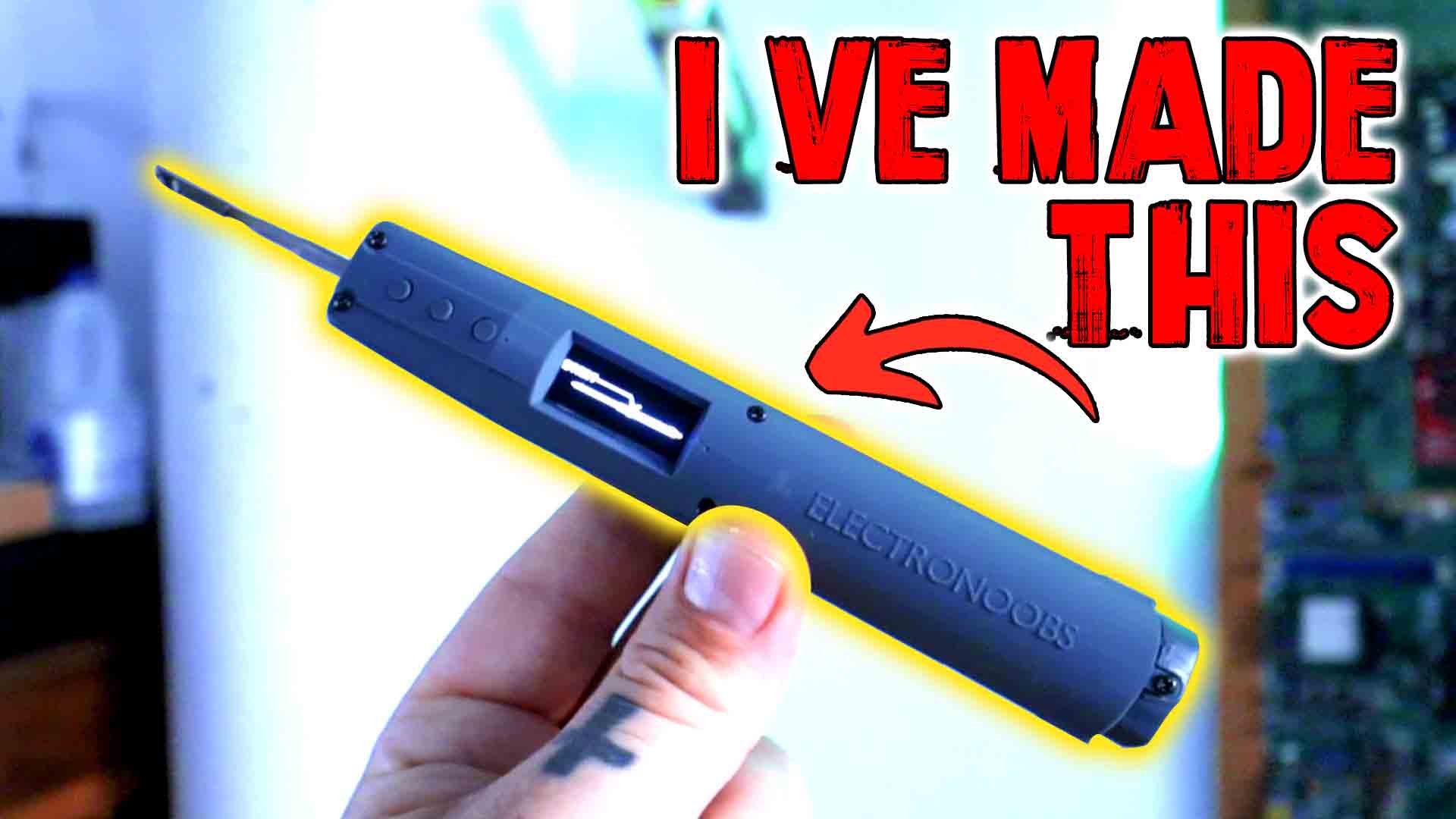
DIY portable soldering iron V3.0
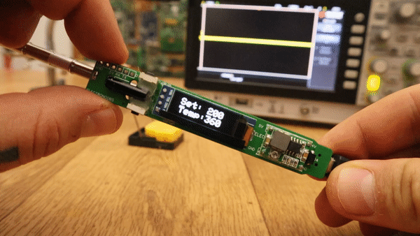
Now we can solder the remaining components such as the vibration sensor and the side push buttons. The board I've made didn't had the wings pads for the buttons, that's why I've put some hot hlue behind the buttons. But the final GERBER file has the wing pads for the buttons so solder those as well. Next we solder the clips for the T12 tip. Make sure the clips are on the bottom side.
Read more
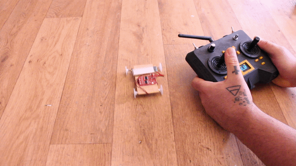
Arduino brushed motor DRONE tutorial
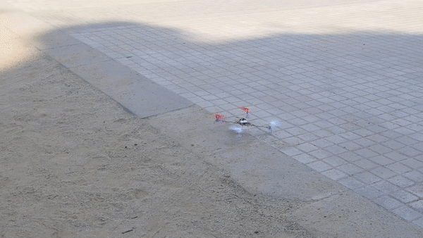
Go step by step and build the ultra low cost drone using some wood sticks, the Arduino, the MPU6050, NRF24 radio modules, the old radio transmitter and last but not least, the cheap brushed motors.. Read more
DIY Smartwatch + Bluetooth
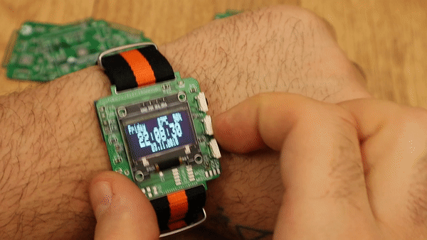
I've been working on an Arduino based smartwatch that could show time, date, alarm, temperature, connect to a smartphone via Bluetooth and show notifications. I had some errors on this baord, but in this tutorial, I'm sharing the good board that I've already fixed. See below all the files, the GERBERS, the code and a step by tep tutorial. Lets start!
Read more
HOMEMADE ELECTRIC LONGBOARD
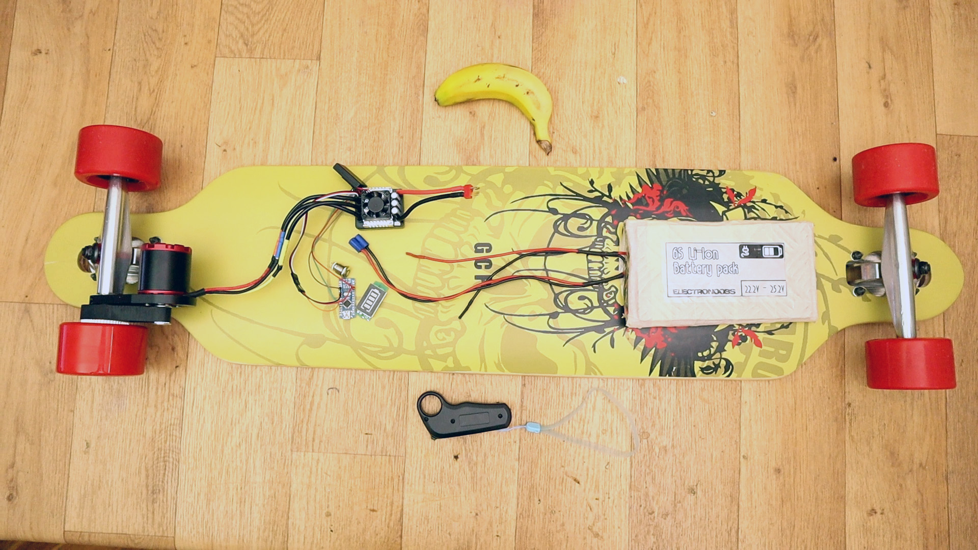
I've started a new project. I want to make my own homemade electric longboard with a powerfull Brushless motor. The first idea was to use two motors, but I had not enough space between the wheels of my longboard. In this tutorial we will see how to mount everything together, make a test and give the final results. Make sure you watch the tutorial on how I've made my homemade 6S battery pack in order to finish this tutorial. Read more