


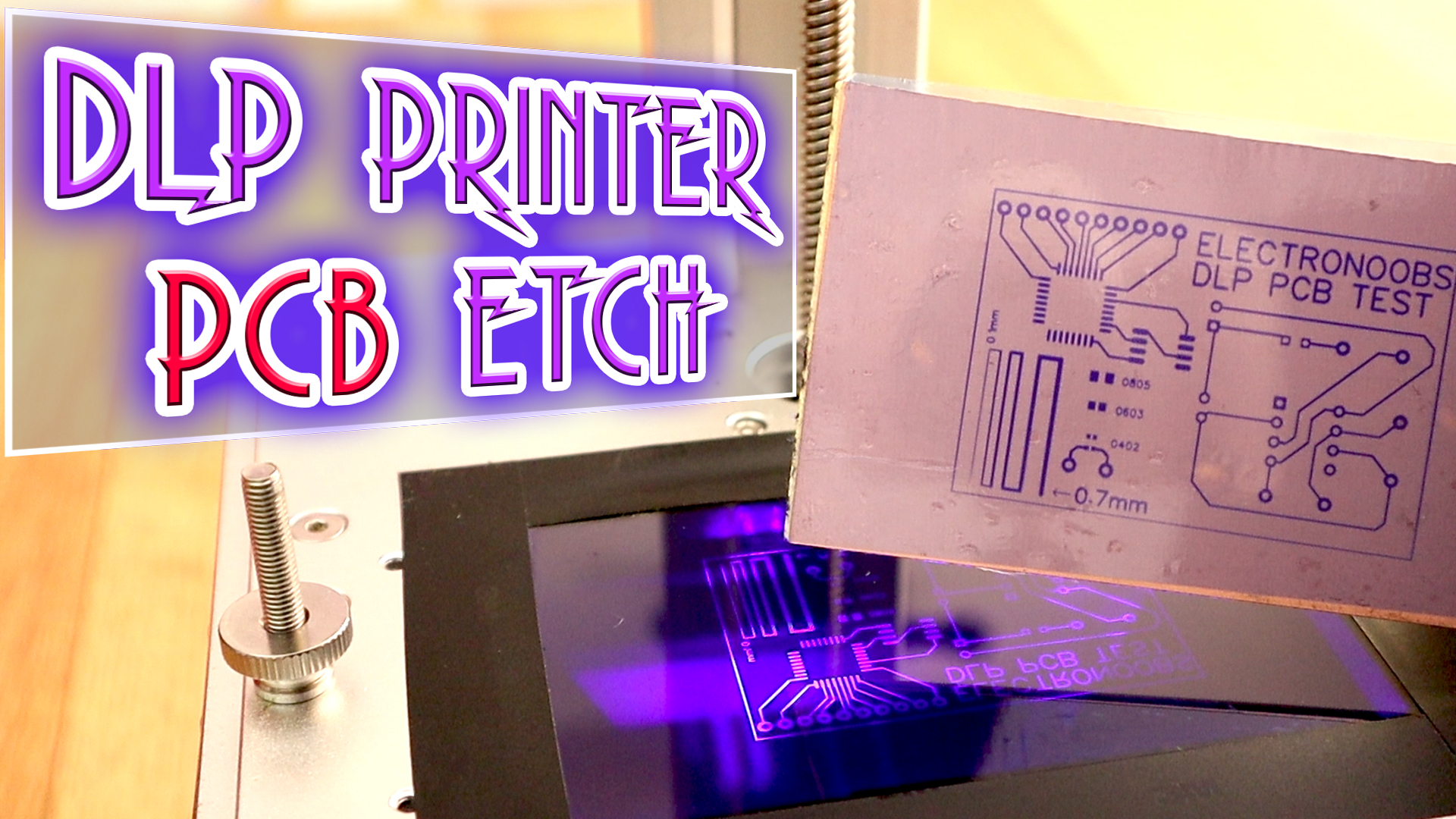
In this tutorial, we will use a DLP printer to expose the circuit layout on a photosensible film over a copper board. Then, we will use acid to etch the PCB and see the results. DLP printer should give us very good results. But first we haev to prepare the 3D file and then etch the PCB.
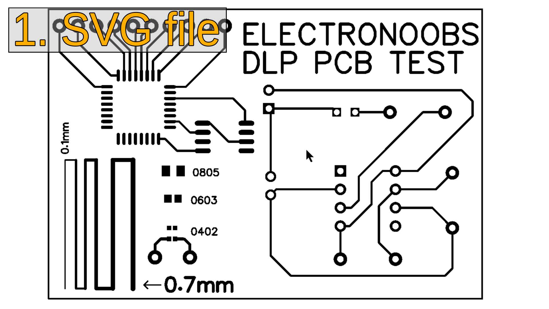
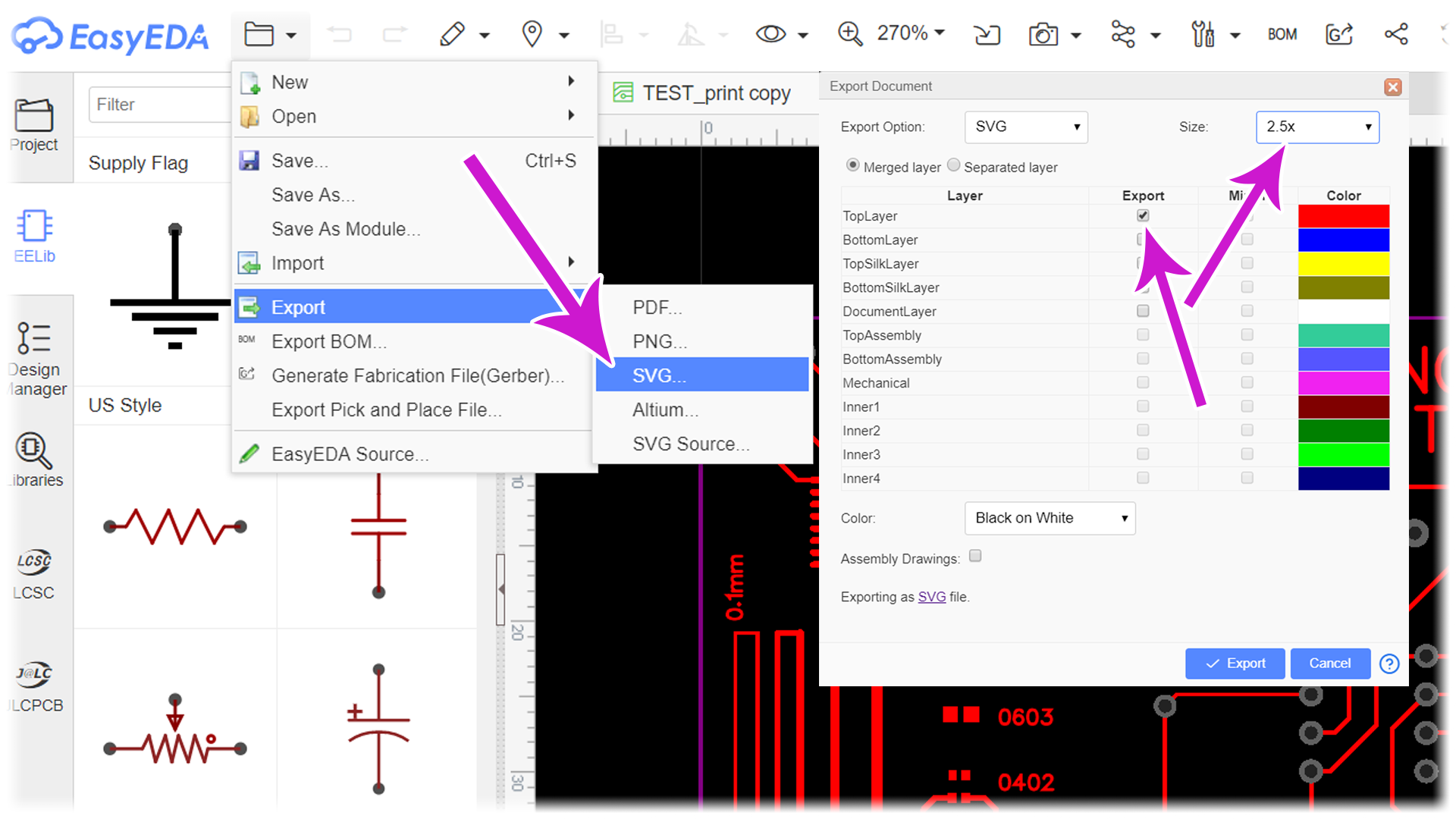
First we need a circuit to print. I've used easyEDA to design my circuits. When you have the circuit ready, save the file and gom to file and select export. There select the SVG type and select only the top copper layer to be exported. Also, select a scale of 2,5X because the bigger the size of the SVG file, the better the resolution of the 3D printable file since that's what we need to create.
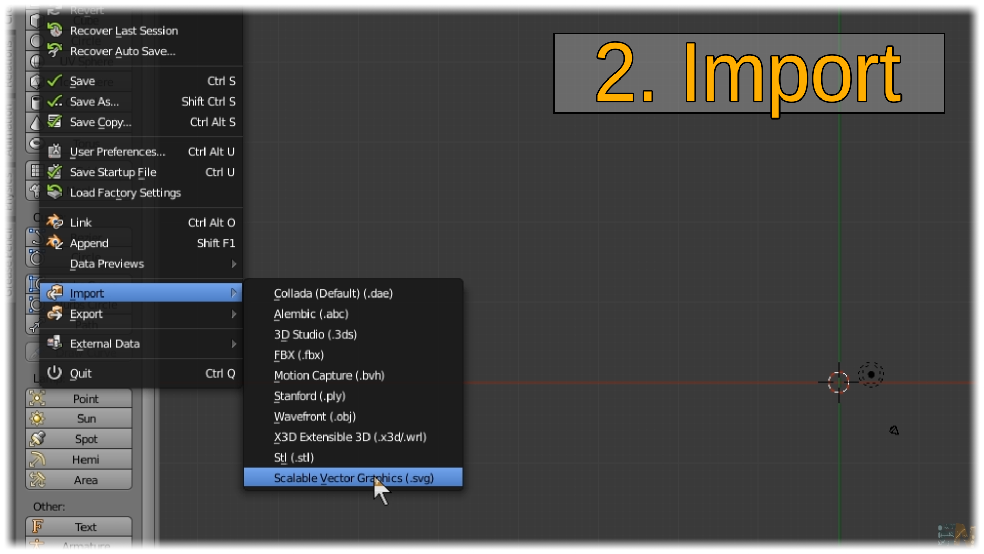
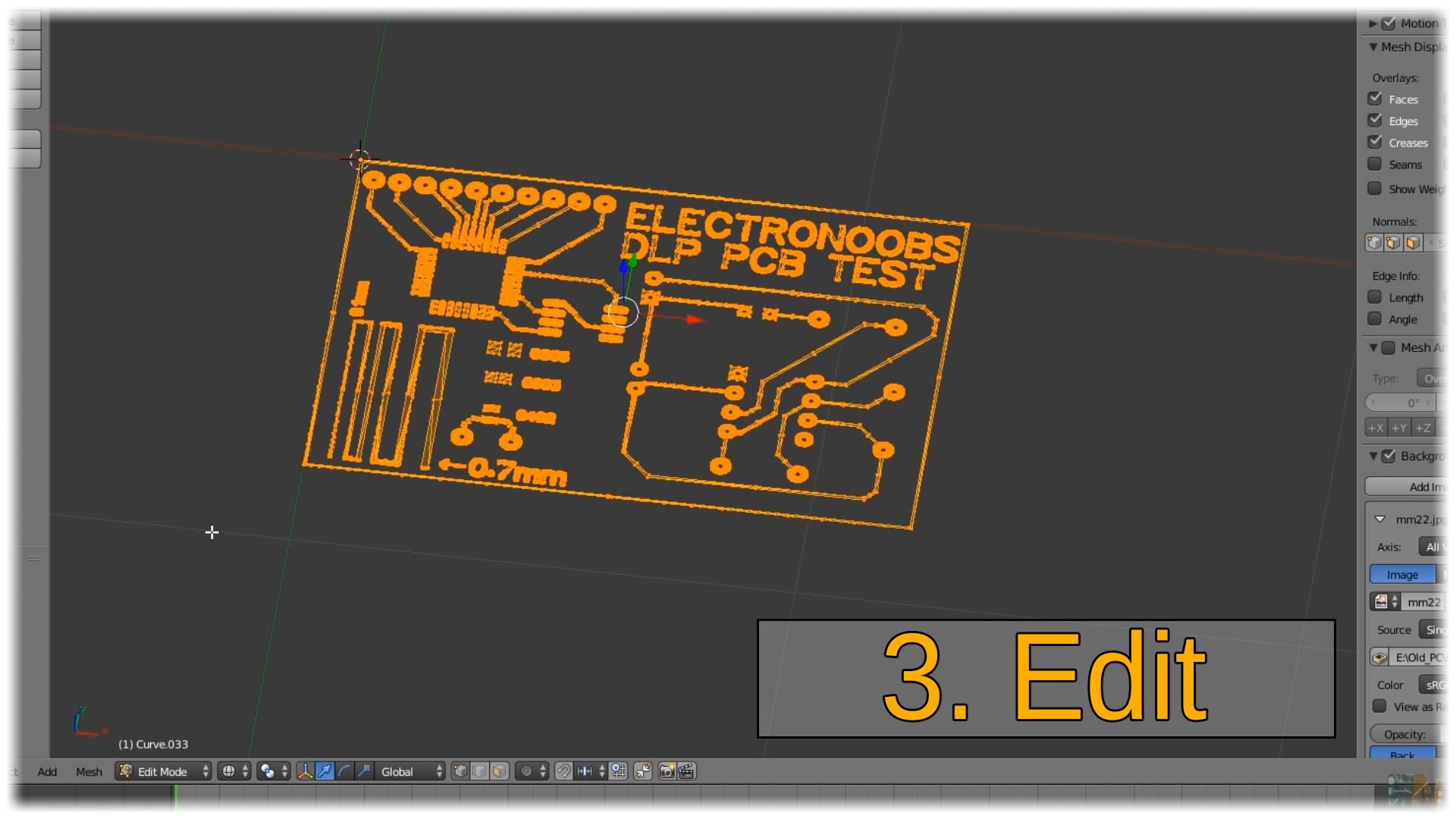
Now that we haev the SVG file, we will use Blender software to create a 3D file. Download free Blender from below and open it. Using this software we could create a 3D file out of the SVG file. For that go to file, import and select SVF file and open the downlaoded file from easyEDA.
Now that we have imported the SVG file in Blender, we need to edit it. You will see that each track is separated. For taht maintain pressed CTRL and with the left mouse click select all the tracks. Now press "CTRL + J" and merge them togeter. But this is not a 3D mesh. For that, select it once again and type "CTRL + C" and select create mesh. Now this is a 3D file. Press "TAB" and enter edit mode and select all the vertices. Now I extrude the file 3mm upwards. Now export the 3D file.
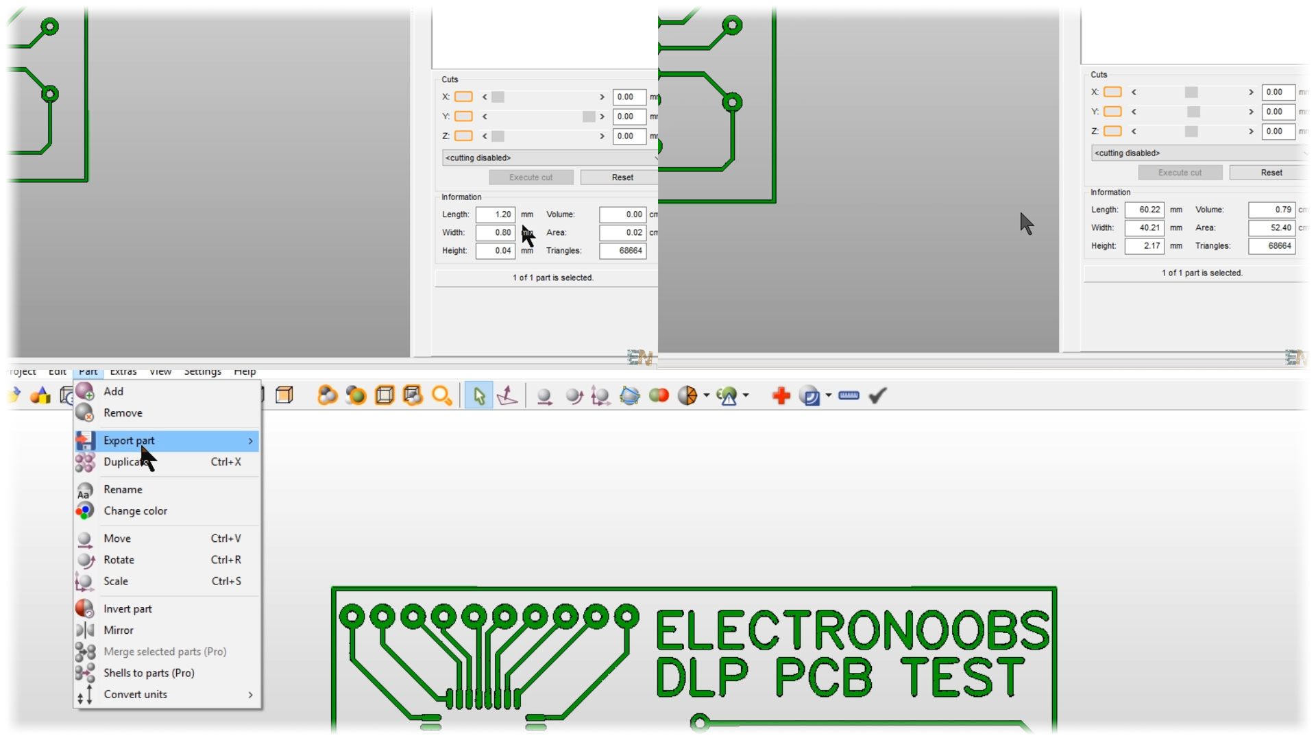
Now download Netfabb from above and install. Open it and import the created 3D file. Correct any error with the "+" icon. If there are no errors check the file size. I know that my baord is 40x69 but as you can se above when I import the file it is 1,2 by 0,8. So, I scalae the file 50 times and obtain 60 by 40mm. Save the file on to the SD card and insert it into the DLP printer
Check the list below in order to know what we need for this. But first, we need a DLP printer with UV light. Take the photosensible film and cut it to the size of your copper board. Then, peal one protective part of the film and glue the film to the copper board. Use a heating iron to glue it well to the PCB. Once that is done, place the PCB with the photosensible film over the DLP printer circuit and let it there around 10 minutes to expose.
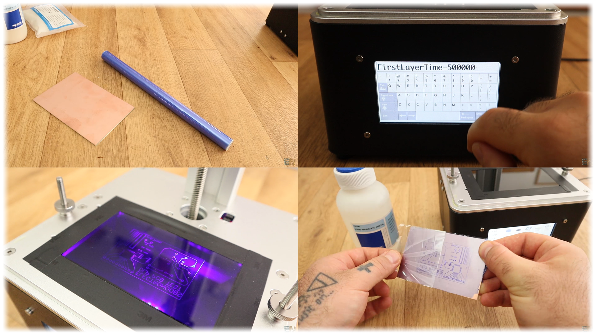
Now that the ciruit is exposed, is time to peal the second protective film. After that we submerge the PCB into water and sodium carbonate. That wikk clean the nonexposed parts of the film and live only the circuit over the PCB.
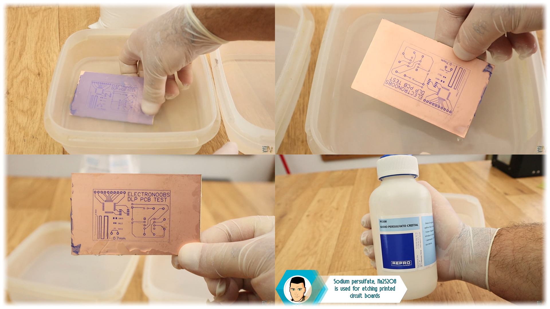
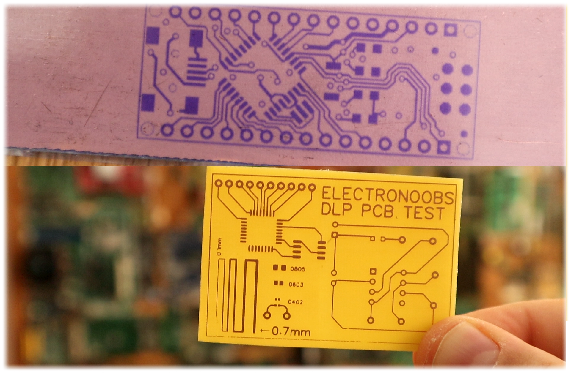
Now clean it under water and put it into the acid bucket. That is a mix of water and sodium persulfate. Move the bucket till all the copper is removed and we are ready. The baord is perfectly etched and with very good details.
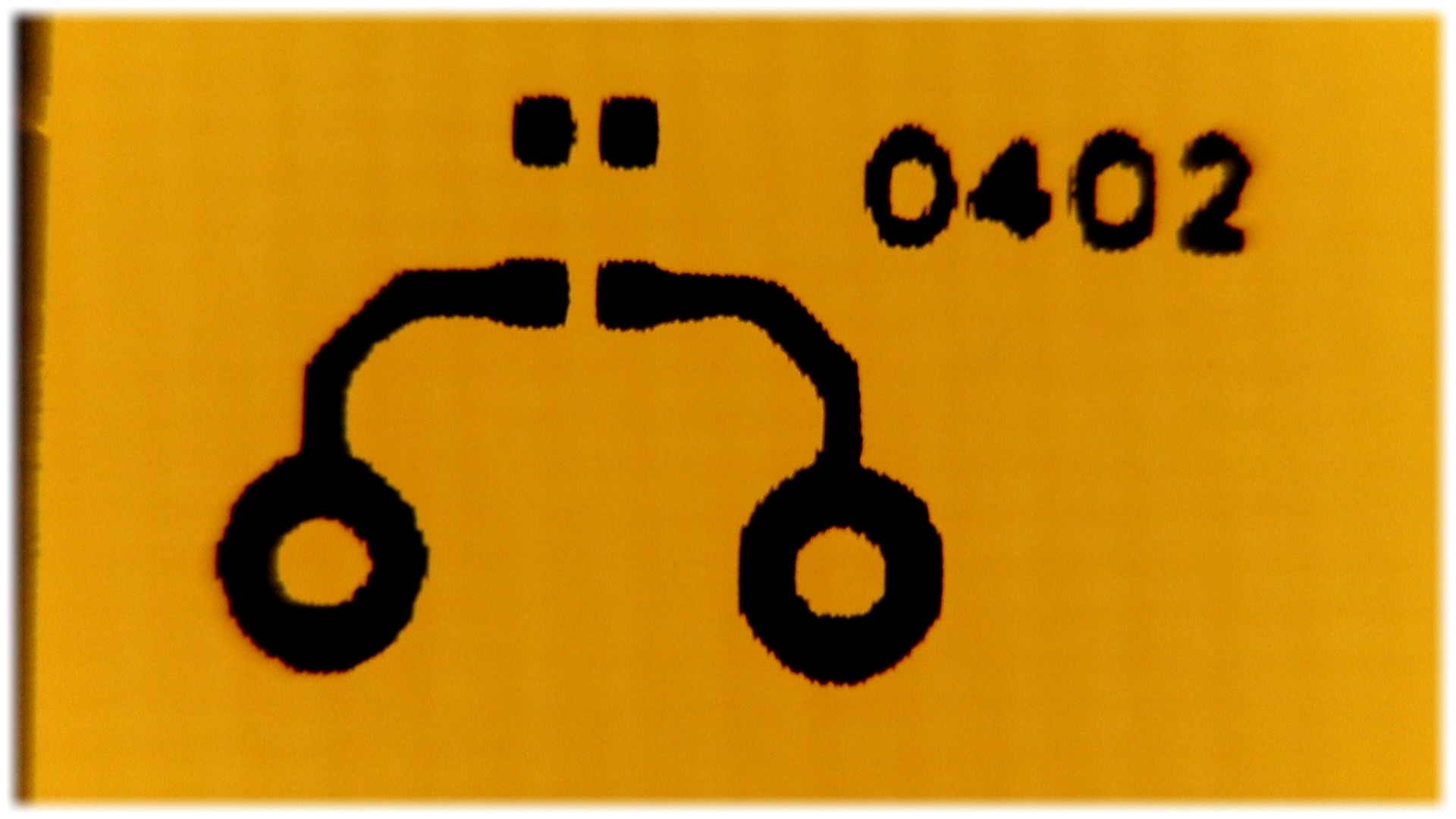
That's it, we ahve sucesfully etched a PCB using a DLP printer. The quality is very good. Even for 0402 size smd components, the pad are very good. I was able to create 0.2mm tracks with no probems. Even down to 0.1mm tracks.