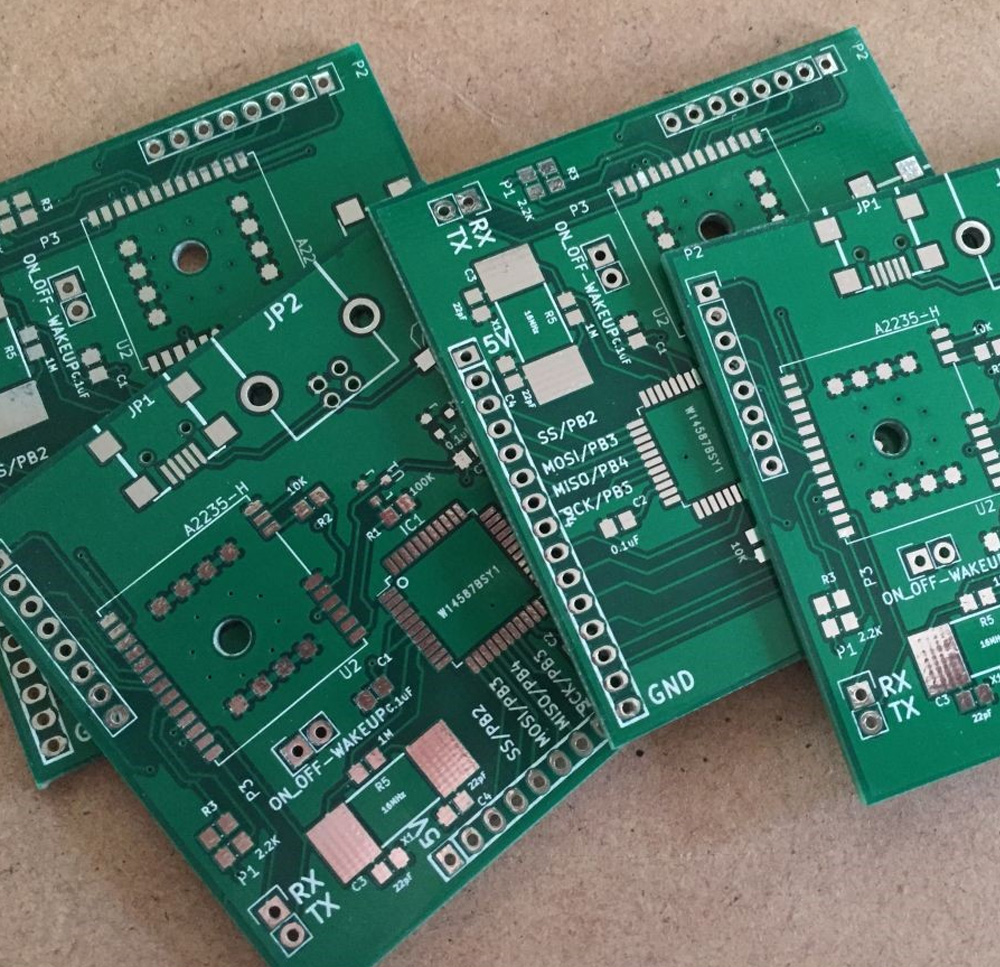
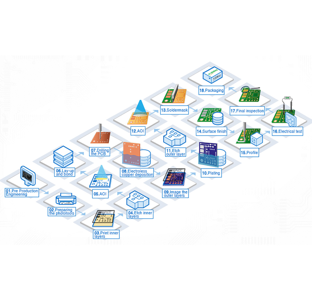
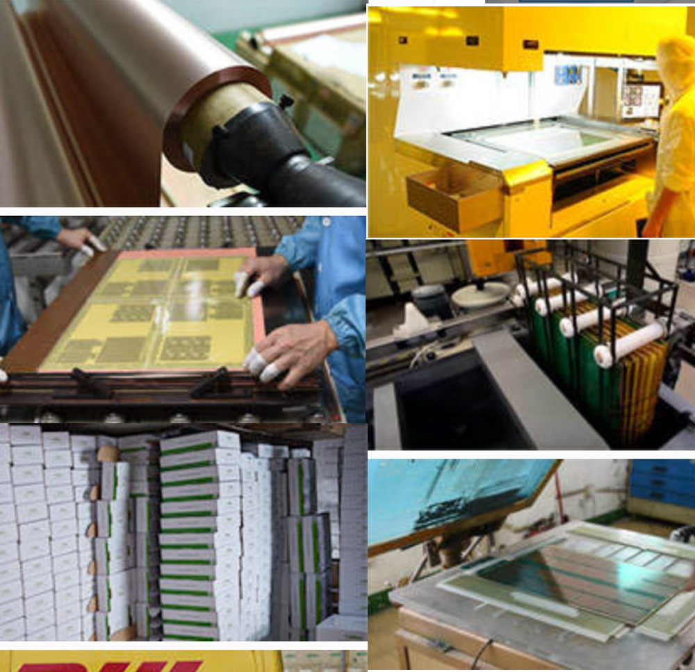
It al starts when PCBway receives the GERBER files of the costumer. These files haev the copper layout, the outline of the board, the place where the holes will be drilled and the silk layer on top fo the PCB. The plain copper PCB is prepared, the copper layer is printed over a mask and then the excess copper will be removed with an acid process. The mask is removed and we get the copper tracks. After each process an inspection is made to make sure the process was done well. Then the holes are drilled with all sizes.
The board gets electrolized and copper is deposited so the inner part of the hole has copper as well. The board is plated wi it will be stronger and it won't oxidise later. The outline is cur and a solder mask is placed over the entire copper part to protect it. The final step is to add the silk layer and packagind plus shipping.
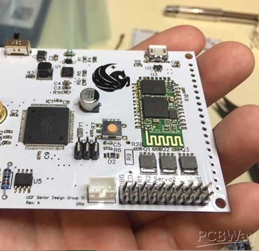
Here are some of the main capabilities of PCBway. PCBs of up to 10 layers, material of FR-4 and aluminum, maximum size of up to 500 by 1100mm, board outline tolerance of 0.2mm, baord thickness of 0.4 up to 2.4mm and min traces of 0.1mm which is great. You can have drill sizes of 0.2 up to 6.3mm and different shape of the PCB outline cut. For the silklayer, characters of less than 0.8mm high will be too small to be recognizable. And for the solder mask color we have no extra charge for (Green, Red, Yellow, Blue).
They accept 5 PCB file formats ( gerber file, .pcb, .pcbdoc .cam or .brd file format) for PCB fabrication. But if you design your boards with Sprint-Layout software, you can send the .lay6 file to service@pcbway.ru for manually generating Gerber files.