Date: 17/07/2018
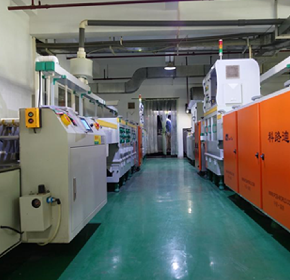
Established in 2006. JLCPCB Factory is the earliest prototype and small-batch PCB production factory in China. Now, JLCPCB has four PCB manufacturing sites. Come with us on a tour of the PCB fabrication process for a 2 layer board to find out how a PCB is made and you will see the care and attention that we give to every step of process, from Production, Quality Control to Shipping.
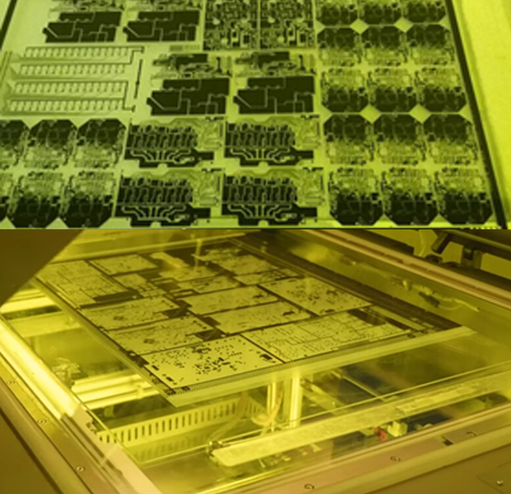
Step 1 From File to Film
After orders are received online on JLCPCB ($2 for 10PCBs), customer supports pass the Gerber files to engineers for pre-production checking. After the file review is approved, the file can be plotted in our laser photoplotters and made into photomasks or films in in a temperature and humidity-controlled darkroom. The photoplotter takes the board data and converts it into a pixel PCB image. The exposed film is automatically developed and unloaded for the operator. The films are ready for the PCB fabrication process
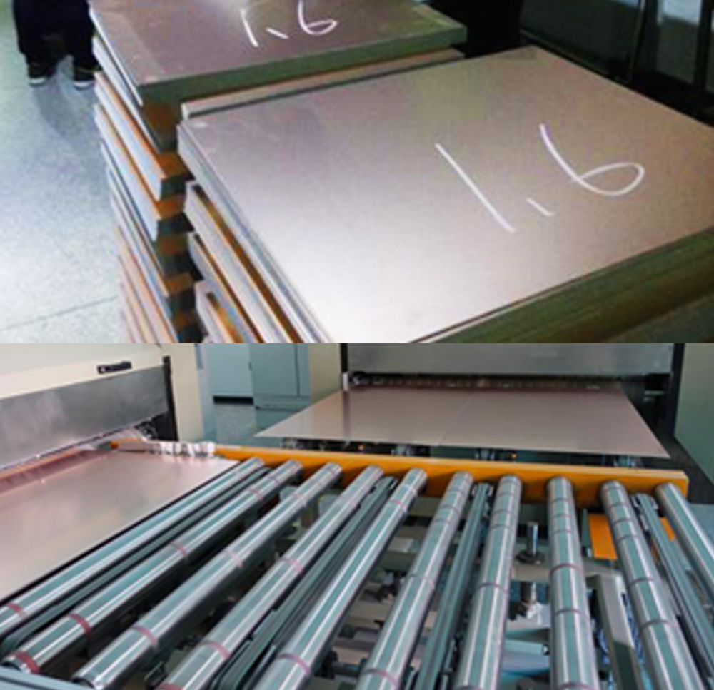
Step 2 Material Cutting
Starting as a large sheet, standard industry quality FR4 in 0.4/0.6/0.8/1.0/1.2/1.6/2.0mm thicknesses with high quality copper foil bonded to both sides - referred to as laminate - is cut to into all kinds of suitable sizes to make panels.
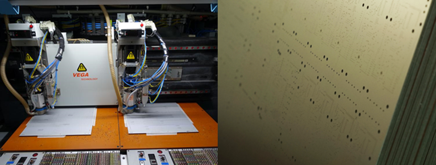
Step 3 Drilling
Holes are drilled through the panel for component leads and vias where specified in the Drill File that EasyEDA generates as part of the Gerber file package. Extra holes are drilled around the edges of the panel to provide registration points to align the photofilms on the top and bottom layers on Step 5. This is to ensure that these pre-drilled holes will then appear exactly in the centre of the pads and vias.
The drill machine is computer-controlled, the worker choose the right drill program which tell machine which drill to use and how to drill on PCB. Many drill machines automatically loads and unload the panels at the completion of each drill cycle in 24 hours every day. There about more than 70 drill machines in one of JLCPCB factory.
Step 4 Copper Deposition
After drilling, the panels are cleaned and then they are placed in baths where, using an electroless deposition process, a very thin additional layer of copper is deposited over the whole panel including an even plating around the walls of all the drill holes to create what are called plated through holes. Almost all PCBs with two or more copper layers use plated through holes to connect the conductors between the layers. The entire process of dipping, plating, washing and drying is machine controlled.
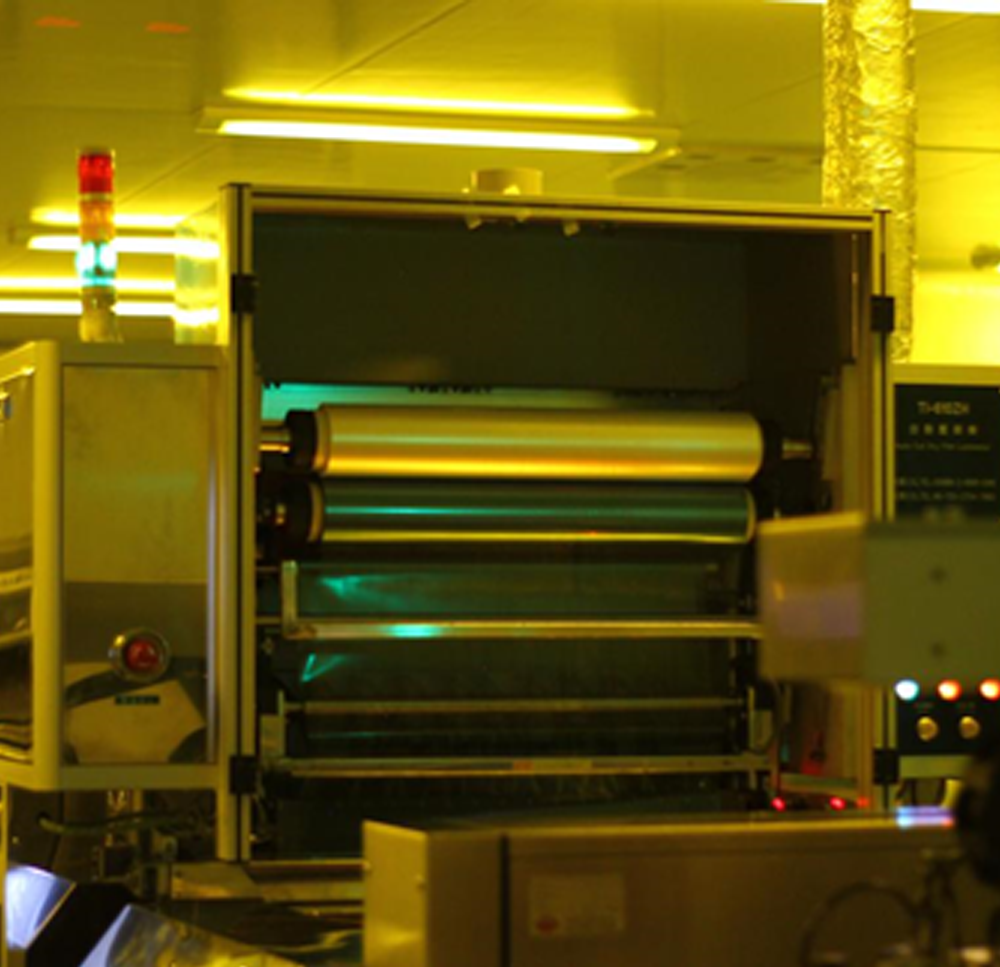
Step 5 Image the outer layers
In the process of Dry Film etching, the whole board surface is first coated with a thin layer of photosensitive etch resist (“photoresist”), as a “dry film”. This resist layer is exposed to ultra-violet (UV) light through a photomask which masks off the required pattern of tracks and pads but allows the whole of the rest of the panel to be exposed to to the UV light. Exposure to UV light polymerises and hardens the photoresist. Unhardened photoresist is removed by “developing” to leave bare copper that will form the required pattern of tracks and pads clean and clear of photoresist. The panel is then baked to increase the durability of the remaining resist for the next process.
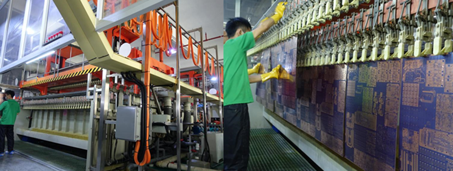
Step 6 Pattern Plating
Following a stage of electroplating to increase the copper thickness on the exposed areas and inside the plated through holes, the exposed areas - again including inside the plated through holes - are then plated with a thin layer of tin. At the end of this step, all the remaining photoresist is removed leaving a panel covered in bare copper with only the tracks, pads and through holes covered in a thin layer of tin.
Step 7 Etching
The tin plating protects the sections of the panel meant to remain covered with copper during the etching stage. Etching removes the unwanted copper foil from the panel but leaves the tin plated areas unetched (apart from a small amount of side etching which is adjusted for by automatically increasing the track and pad widths to compensate during the original photomask preparation in Step 1).
Next, the tin plating is chemically removed in a process that re-exposes the bare copper. so that the conducting copper areas, tracks, pads and through plated holes are now all that is left of the original overall copper coating on the panel.
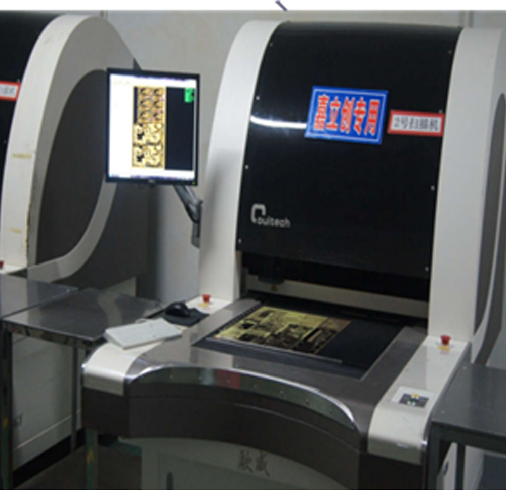
Step 9 AOI Inspection
Automated optical inspection(AOI) is an automated visual inspection for bare boards. An AOI is able to detect faults such as tracks with over etched edges or regions where the photoresist may have been scratched or chipped and so caused a notch in the track. Faults such as this are very hard to detect in an electrical continuity test.
The AOI system scans the layers using a laser sensor. The captured image is digitised, enhanced and then electronically compared with the original Gerber file. Using this comparison the AOI system is able to detect and highlight any defects or suspect areas far more swiftly and accurately than a manual inspection.
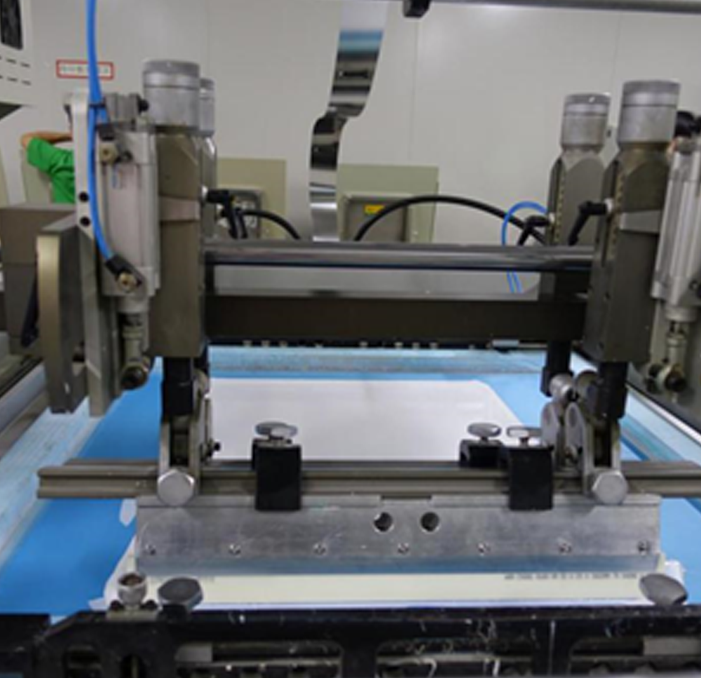
Step 10 Solder Mask
Solder mask is an epoxy coating applied to the bare printed circuit boards to prevent accidental solder bridging and protect them from the environment. Solder mask is usually green but many other colors are available, such as red, black, white, yellow and blue. After another stage of cleaning, panels are loaded into the solder mask coating machine. This completely covers both sides of panel with an solder mask ink. The panels are then put through a drier which hardens the ink just enough to allow it to be printed. Next the “tack-dried” coated panels are imaged under UV light using a set of photomasks which, before exposure to UV, are checked to ensure that they are precisely aligned (to better than 50um) with the copper tracks and pads on the panel. The photomasks are clear where the solder mask is to be further hardened and opaque where the solder mask is to be washed away in the “development” stage to expose the pads on the panel.
The development stage strips off the unhardened and unwanted resist. To ensure that the exposed copper is ideally solderable, the panels are then inspected to ensure that there is no residual ink left on the pads or through the holes. Even slight traces would compromise the solderability of the finished PCB. Lastly, the resist will be further hardened or “cured” to provide a permanent, hardwearing coating
Step 11 Silkscreen
Silkscreen guides customers to better understand the board’s component layout.
In an automated process, Letters, numbers, logos, production date and component outlines, as defined by the silkscreen layer file of the Gerbers, are printed on the top surface of the panel, using a white etch-resistant ink printed onto the board using a special type of ink-jet printer. If silkscreen is required on the bottom surface then the top surface ink is tack-dried before the board is turned over and the printing process repeated using the bottom side silkscreen file.
The panel is then cured again to finally harden off the solder mask and silkscreen inks.
Step 12 Surface Finish
During this stage, boards are plated with an electroless-gold-over-nickel (ENIG), silver or hot-air-solder-leveled surface. The surface finish has two essential functions, to protect the exposed copper areas from corrosion and to provide a solderable surface when assembling (soldering) the components to the printed circuit board.
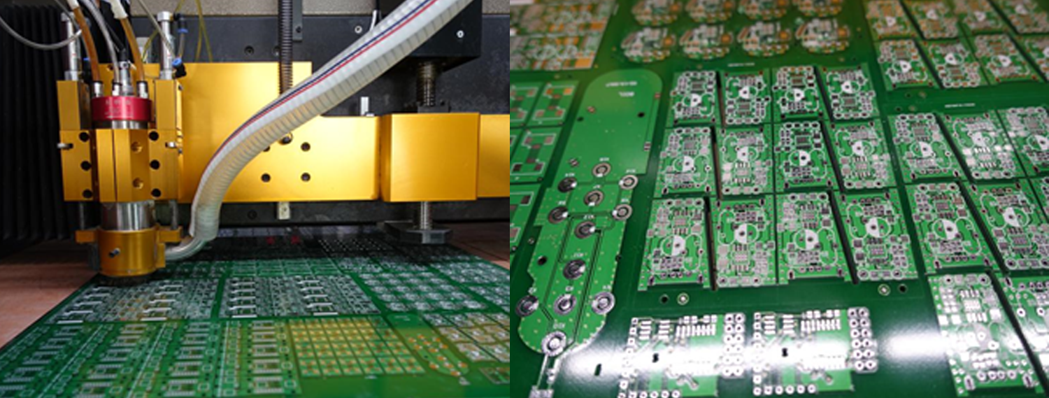
Step 13 Profiling & V-cutting
After surface finishishing, panelized boards need to be shaped to suit enclosures via a computer-controlled milling or routing machine. With profiling, boards were usually finished to give a smooth edge once they are cut. Fast profiling methods allow the PCBs to be laid edge to edge and so gives the best panel utilisation.
V-scoring/V-cutting is used for mechanical pre-separation of circuit boards. A V-shaped breaking line is formed in the circuit board with a precision cutting tool. This breaking lines permit the boards to easily be snapped out from the panel.
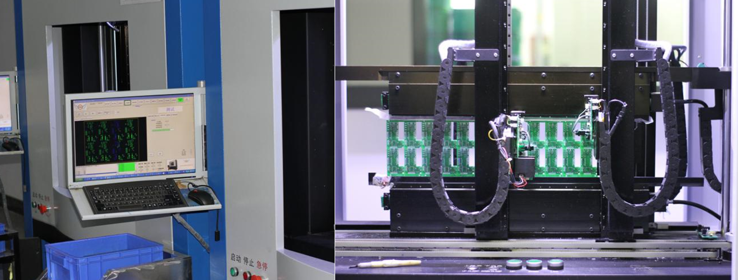
Step 14 Electrical test
We electrically test every multilayer PCB against the original board data. Using a flying probe tester we check each net to ensure that it is complete (no open circuits) and does not short to any other net.
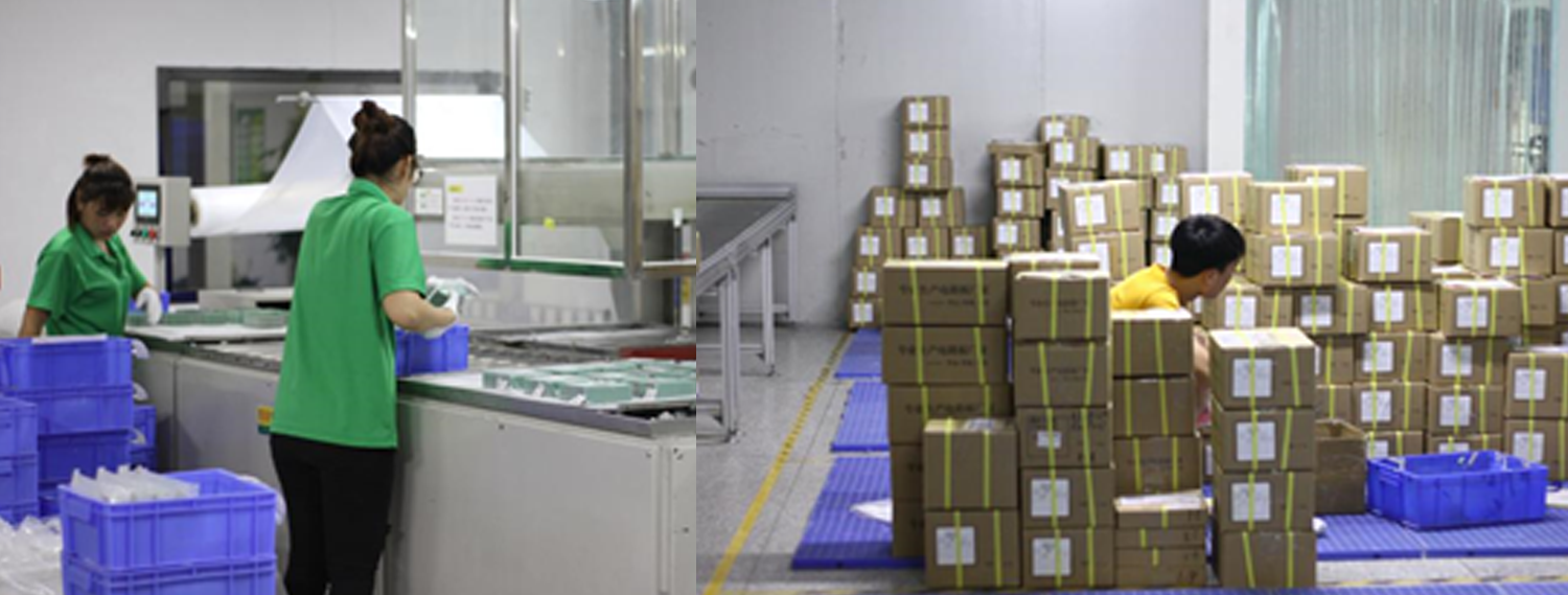
Step 15 Final Quality checking & Package & Shipping
All PCBs produced by JLCPCB are given an electrical connectivity test and a final visual inspection to ensure everything is OK before being packed and shipped.


 See other blog→