


Finally, the board works perfect. So I could make a 3D design for the case and this is a final product that could end up on Kickstarter. It is a very cheap project, around 15$ for all the parts . On this tutorial you willhave a full part list, the schematic and layout of the board in case you want to amke it. I also share the 3D STL files for the case so you could print it.
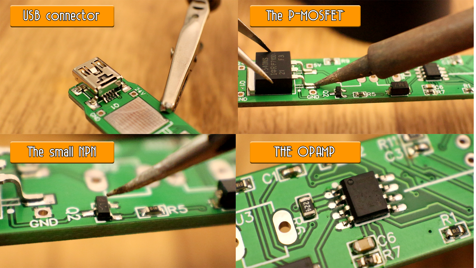
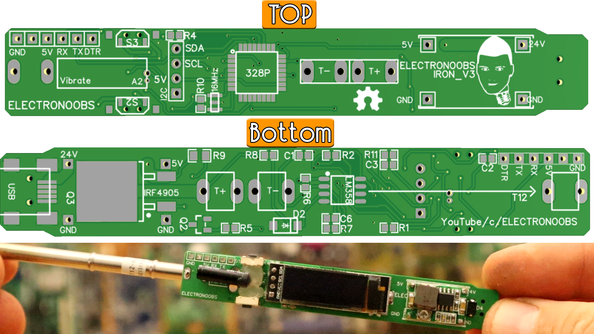
Below we have the schematic for this board. To supply it we use a type mini B USB connector. That is connected to the power MOSFET but also to some pads for the buck converter so we could get 5V for the other microchips. Now the 16Mhz crystal is smaller so we have more space on the PCB for future improvements. See version 2 to see the other PCB. We haev 2 push buttons to set the temperature and other settings, a vibration sensor for the sleep mode and the ATmega328p.AU microcontroller. See full part list for all the components.
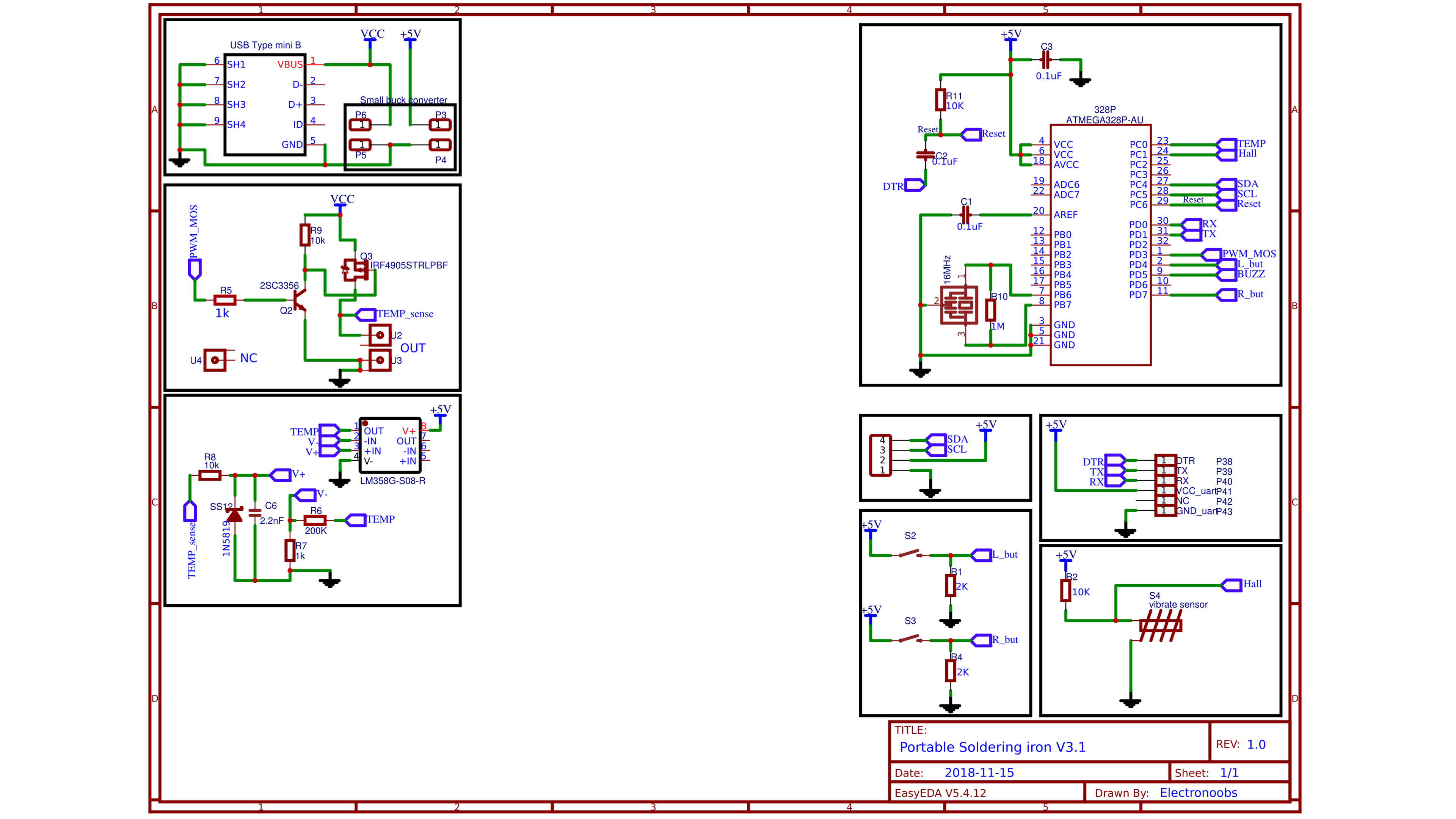
There are a few more pads for the UART connection so we could program the board. See that the board has no SPI connection, so the ATmega328 chip must have a bootloader, otherwise we won't be able to burn one later. This should be a improvement for future boards. Now let's see the layout.
Below you have a picture with the top and bottom side of the PCB. You can see that the tracks on the input are very thick, 2mm in this case since those will have to withstand currents up to 2 or 3 amps from the input to the MOSFET and T12 tip connectors. Below you could also see a real distribution of the real PCB. To secure in place the T12 iron tip, I've used some PCB fuse clips. Those will be soldered in the middle of the PCB on the bottom side and that is the side that has the LM358 OPAMP. The buck converter must be soldered on the top side and the OLED screen as well. The rest are SMD so they can only be soldered on one side so there shouldn't be any problem.
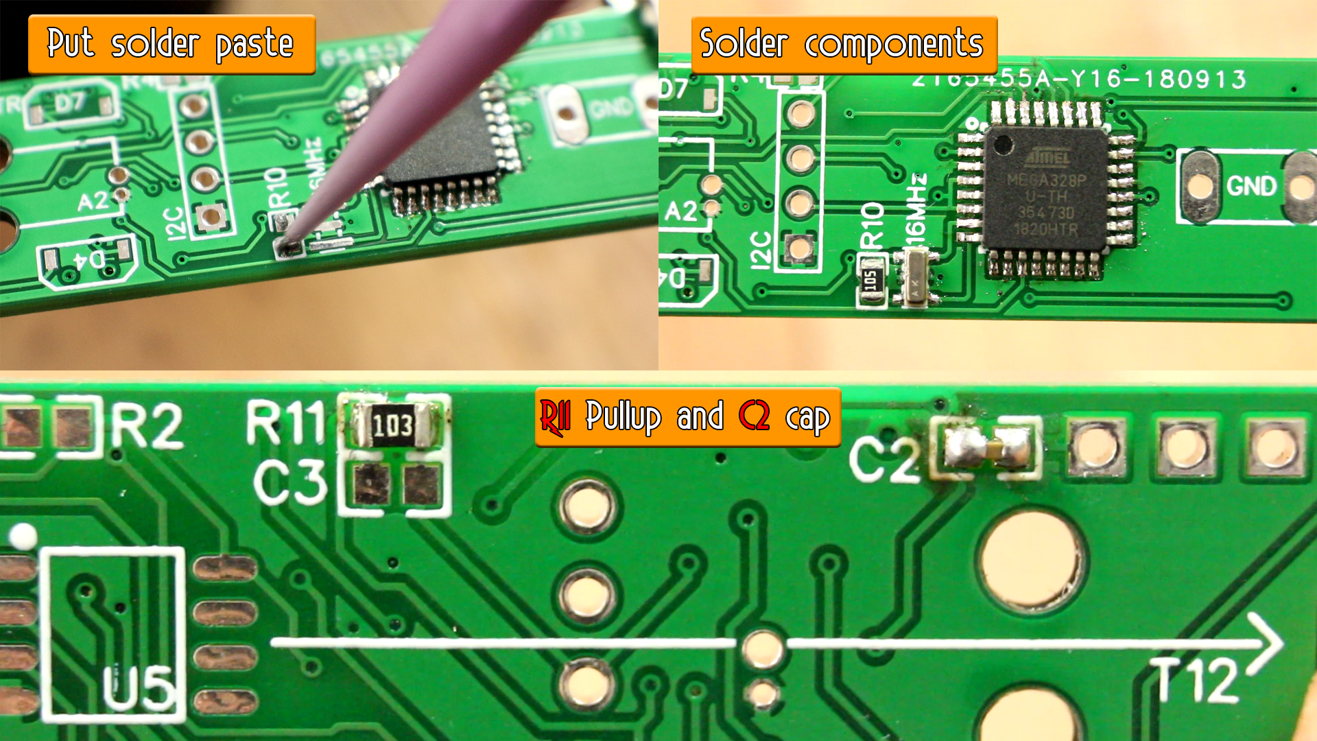
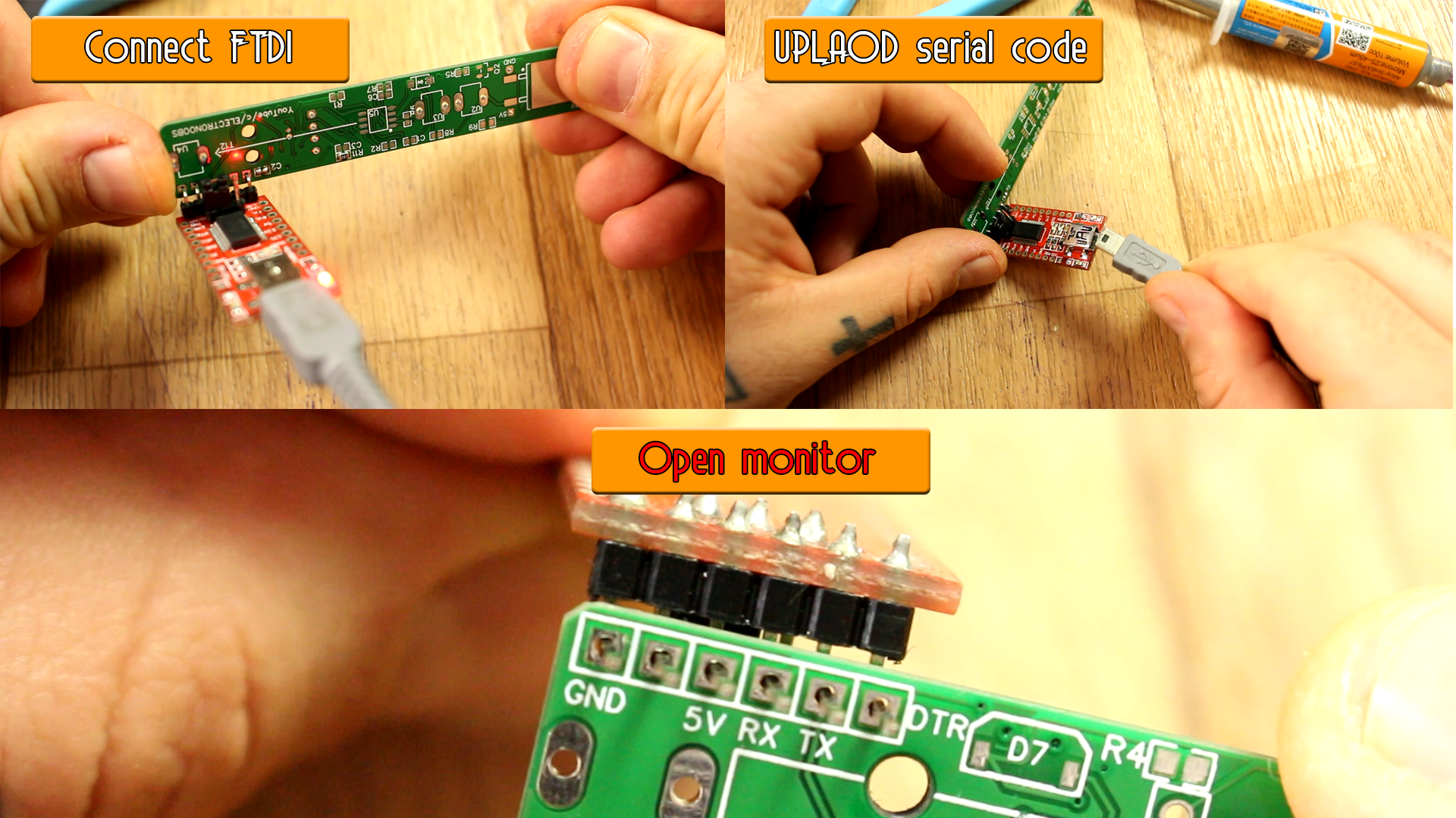
With these components, the chip should work. The 10K pullup will keep the chip active, the 16Mhz crystal will create the clock signal and the C2 capacitor is used to reset the chip with the DTR pulse. To test if it works, we have to connect an FTDI module an the UART pins. I then upload a test code that will write numbers on the serial monitor. Open the monitor and if you receive data, then the chip is ok and se can keep soldering components.