


What’s up my friends. Welcome back. We will finally learn a bit about the FPGAs, how they work and how to program them. But first, since FPGA stands for field programable gate arrays, we should start from the beginning and first learn what are logic gates.
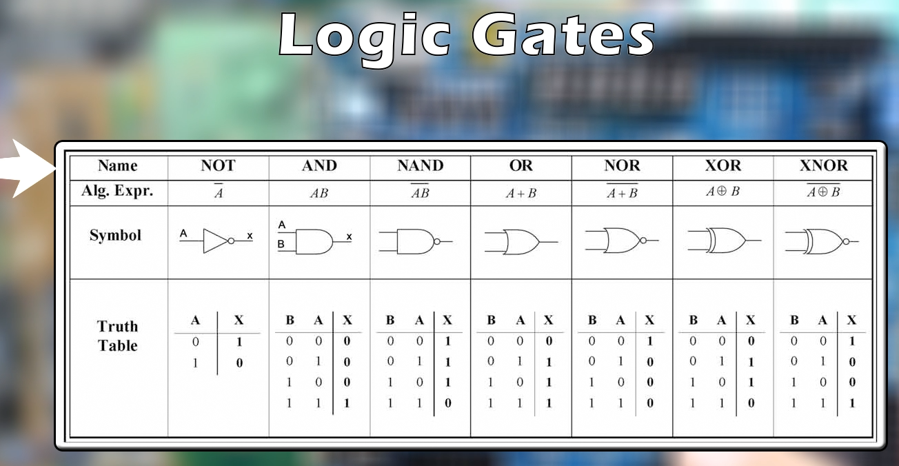
Here below we have a table of the most commune logic gates. This is the name of the gate, how we writhe the function on paper, the symbol of the gate and the truth table.
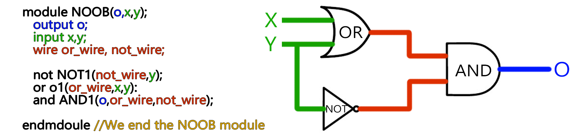
Before anything, I would like to show you why we should know logic gates. Imagine a module taht has 2 inputs, X and Y and one output, O. The output, O, has the next function wehre we can see it is the input X OR Y and an AND between that result and the negative of the Y input.
This transalted into verilog, which is not a programming language but a hardware description lanuage will be translated to the next photo below. The text on the left shows how the HARDWARE into the FPGA will be arranged, not what they do but how are they placed and connected one to each other. So it is importatnt to know what each of this gates do in order to program a FPGA.
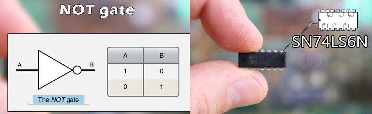
The most-simple is the NOT gate or sometimes called inverting gate. The output of this module is inverted to the input. Each time you see a circle at the output of a gate or a bar on top of the logic function, that means that the gate is inverted. Below I have the SN74LS6N not-gate integrated chip. It has 6 inverting gates inside. Now in digital, logic signals are ones and zeros where zero is the lowest value and 1 is the highest. We will work with ground and 5volts.
As seen in the truth table, the output B is the inverted of the input A. So when we haev for example a 5V input the output will be GND and wehn the input is GND, the output will be 5V.
Next, we have the AND gate and this below is the symbol for this module. Now we should learn what a truth table is. I know this is very basic, but if you are new to logic gates, you will definitely need to know about truth tables. This table below will show the output value according to the combinations of the inputs. In case of the inverting gate, it’s simple. When the input is low, the output is high and vice-versa. Now in case of the AND we have two inputs or more and only one output and this is the truth table for this module. When any of the inputs or both are low, the output will be low. Only when both inputs are high the output is high as well. No matter how many inputs has your AND gate, the output will be high only when all of the inputs are high.
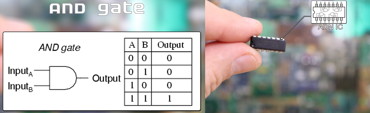
Above I have the CD4081BE integrated chip that has 4 AND gates. I supply 5 volts and ground, connect a LED to the output and add a pulldown to each of the inputs of the first AND gate. Then I connect one push button between the inputs and 5V. Each time I press one of the buttons the input will be high and low the rest of the time.

You could buy one with more inputs or just merge two double input ANDs together and make a 3-inputs one, or 4 or 5 or any amount of inputs but you should know that this combination will add a delay each time we add a new gate in series.
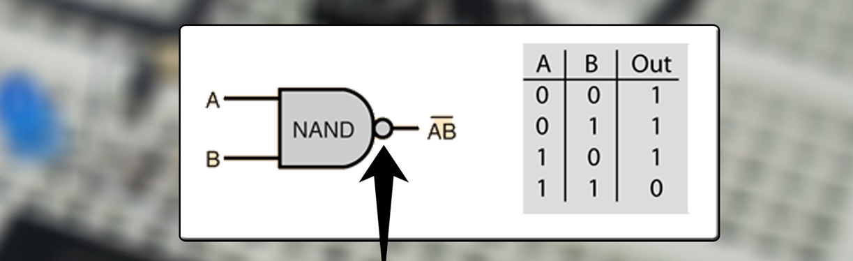
The next gate is very simple. Is the same AND gate but with inverted output as you can see with the circle here. Meaning that the truth table is reversed. In this case the output is always 1 and 0 only when both inputs are high.
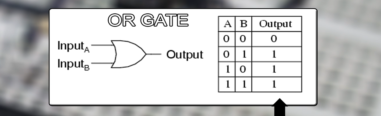
Next, we have the or gate. As the name of this module, the output will be one input or the other. This below is the truth table of this gate and as you can see, each time any of the inputs is high, the output is high as well. Doesn’t matter if we have 5 inputs at low and only one high, if one of the inputs is high, the output will be high as well. For this example, I’ve used the 74LS32 chip that has 4 OR gates. Supply 5 volts and ground and add the push buttons at the input just as in the other examples. Any time any of the inputs is pressed, the output is high.

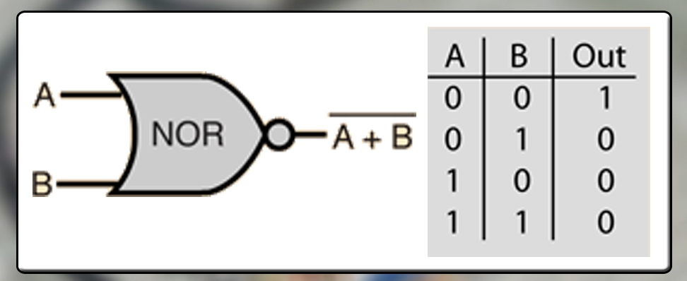
The NOR hate is the same but with inverted output. You could create a NOR or a NAND or any inverted gate just by placing a NOT gate at the output of any gate.
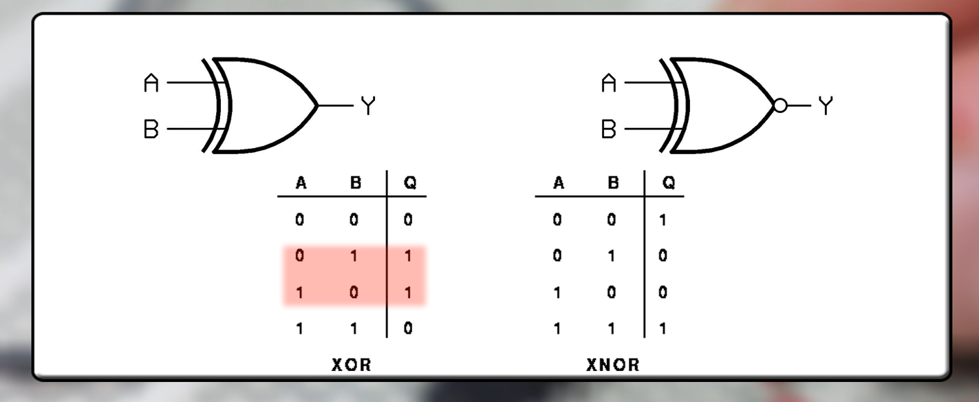
Finally, we have the XOR and XNOR gates and with this truth table. For the XOR gate the output is low any time all of the inputs are the same. If the inputs are different, the output low and in case of the XNOR, well just the opposite.
Ok, guys so now we know the most basic logic gates but what we can do with these gates? Ok so here I have the 74HC574N chip and this is a so-called flip flop. Now we have 4 basic types of flip flops. We have the set/reset one or so-called SR, we have the JK, the D and the T and this are the excitation tables for each one of them.